Appendix B A Hardware Implementation
It is a tradition of our laboratory to implement our
designs as actual hardware prototypes, rather than limiting ourselves to
software simulations. In many cases, this approach has led us to identify
problems and possible improvements which were not apparent in simulation.
Such was the case, for example, for the MicTree prototype described in
subsection
2.2.4, which revealed the limitation of fixed-size cells. To a lesser
extent, designing a prototype of our FPGA also revealed some ways to improve
on our self-replication and self-repair mechanisms.
In this appendix, we will describe the logic layout of
our MuxTreeSR (for MuxTree with self-repair) prototype (section
B.1), and then cursorily describe the MuxNet (for network of MuxTreeSR
elements) circuit (section B.2), an attempt to implement
a 4x4 array of MuxTreeSR elements into a single commercial FPGA.
B.1 MuxTreeSR
In this section, we will describe in detail our prototype
of the FPGA we developed in this thesis. After a brief overview (subsection
B.1.1) of the system, we will present the logic layout of our circuit
following a top-down approach: starting from the cellular automaton used
for replication (subsection B.1.2), through the logic
required for rerouting the array in the presence of faulty elements (subsection
B.1.3) and the state machine which control the array's operation (subsection
B.1.4), to the actual core of the MuxTreeSR element, consisting, as
we have seen, of a programmable function (subsection B.1.5),
a switch block for long-distance connections (subsection
B.1.6), and a configuration register (subsection B.1.7).
B.1.1 Overview
Our laboratory's teaching activities include a number
of laboratory sessions aimed at introducing the principles of logic design.
In order to accomplish this task, we use a set of logidules(logic
modules), plastic cubes which contain standard logic circuits (AND gates,
RAMs, etc.). These modules can be connected together (not unlike a puzzle),
automatically providing the circuits' power supply as well as the minimal
connections between modules.
Aside from being an invaluable teaching tool, the logidules
are also an interesting platform for the development of prototypes, as
they can be easily exploited for the support circuitry which invariably
surrounds any prototype. It is therefore not surprising that we decided
to exploit the same approach in the design of the prototypes related to
the Embryonics project, which we call Biodules (for biologically-inspired
logic modules). The prototype of MuxTreeSR, the FPGA presented in
this thesis, is no exception, and was embedded in a module called Biodule
603 (Fig. B-1).
Each Biodule 603 is designed to contain a single MuxTreeSR
element, along with four copies of the cellular automaton used to define
the blocks' membranes (the four copies were required in order to be able
to use all the Biodules, as explained below in subsection
B.1.2). The Biodule 603's displays include:
- four 7-segment displays (in the four corners)
which show the state of the corresponding CA elements;
- a set of five 7-segment displays which show
the value of the element's configuration;
- a set of four LEDs (top and bottom) used to
indicate the source of the signals (in case of reconfiguration);
- two sets of LEDs which show the value of the
functional outputs and the input and output values of the flip-flops of
each of the two copies of the element's programmable function;
- a single LED which lights up whenever a fault
is detected in the element;
- a three-color LED which denotes the state of the
element (green for active, red for dead, yellow for spare or during the
configuration and repair processes).
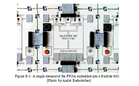
In addition to the displays, each Biodule 603 also contains
a rotary encoder used to select one of ten possible faults to introduce
in the element, and a push-button which activates the selected fault: a
single push will introduce a temporary fault (which will disappear whenever
the FPGA is reset), while a double push will introduce a permanent fault.
Invisible to the user, the Biodule 603 contains a small
printed circuit board on which all the required circuitry is mounted. Aside
from the displays mentioned above and the components (such as resistor
nets) required for their control, the only "active" circuits are a Xilinx
XC4013PQ240-4 FPGA [111], used to implement
the MuxTreeSR element, and a 256k-bit EEPROM used to store the Xilinx's
configuration bitstream.
Using a Xilinx FPGA with a locally-stored configuration
to implement our elements allows us the opportunity of upgrading our design
at a latter date without needing to build a different set of Biodules.
In fact, the amount of programmable logic offered by the Xilinx chip is
much greater than that required to implement our MuxTreeSR elements: our
design uses approximately 15% of the available resources, a figure which
includes all the circuitry required to control the displays. On the other
hand, the XC4013 is the smallest Xilinx circuit available with enough I/O
pins to satisfy our requirements: our design occupies only a fraction of
the programmable logic, but uses 100% of the available pins.
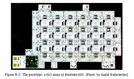
Like all logidules, the Biodules 603 can be joined together
to form a two-dimensional array (Fig. B-2), with the
connections implemented either through the automatic contacts on the perimeter
of the box (8 per side) or through four 16-bit-wide connectors. As of now,
18 modules are available, allowing us to build a 6x3 array of MuxTreeSR
elements.
To operate the array, the following signals must be provided
externally:
- a configuration bitstream, including the input
sequence for the cellular automaton, the test pattern, and the blocks'
configuration;
- two clocks, a faster one for the configuration,
and a slower one for the operation of the array;
- a functional reset, which resets the elements'
flip-flops to the default value defined in their configuration;
- a global reset, which resets the current configuration
of the MuxTreeSR array;
- a power reset, which resets the configuration
of the Xilinx chips.
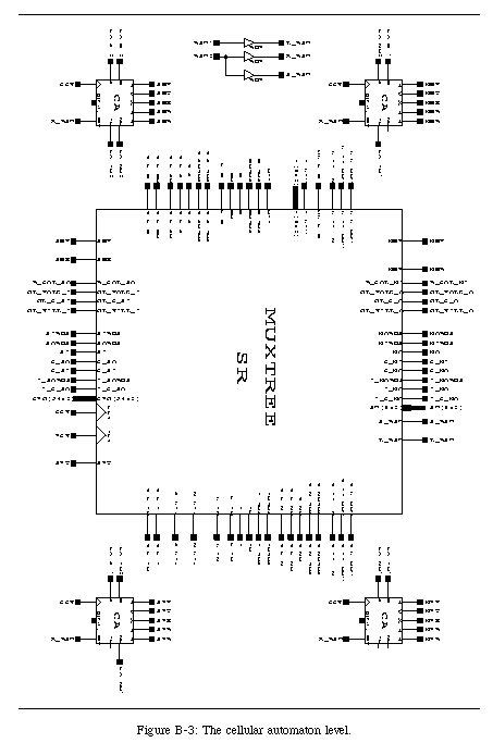
B.1.2 The CA Level
The topmost level in the logic layout of our element
is, of course, the interface between the I/Os of our element and the pins
of the Xilinx chip. With a few exceptions (e.g., the encoding/decoding
of the signals controlling the 7-segment displays), this relationship is
one-to-one (i.e., a pin for each I/O line), and is therefore of no particular
interest.
The topmost relevantlevel in our layout is therefore
the cellular automaton which defines the size of our blocks (Fig.
B-3). As we have seen, the CA elements are placed outside of the MuxTreeSR
elements (Fig. 3.29), and in theory a
single CA element per Biodule would be sufficient to realize our system.
However, since each Biodule contains a single MuxTreeSR element, and since
the CA membrane must completely surround the active logic elements, we
were forced, in order to avoid "wasted" modules, to introduce four
CA elements into each Biodule. This redundancy, which is not crucial since
we use only a fraction of the Xilinx's programmable logic, allows us to
obtain an usable logic element for every available Biodule.
Our first implementation of the cellular automaton was
functionally equivalent to the automaton described in section
3.5, which allowed a fairly trivial transition to hardware. We soon
realized, however, that the limitations imposed by this automaton (notably,
the requirement that blocks be perfect squares) were too restrictive, and
we improved its functionality to that described in subsection
4.3.3. The new automaton allows both the definition of rectangular
blocks and the assignment of spare columns of elements. Unfortunately,
this improved functionality comes at the cost of augmented complexity,
and the hardware implementation of the new automaton is far from trivial.
As we have seen in section
A.2, the new automaton uses 23 states and a neighborhood of 5, with
a total of 207 transition rules. A trivial implementation of this automaton
would require a look-up table of 235 5-bit
words, a 5-bit register to hold the present state, and eight sets of 5-bit-wide
connections with the neighboring elements (four input and four output busses).
Even if it were possible to reduce the size of the look-up table (since
the automaton uses a fraction of all possible transition rules), such an
approach is obviously out of the question, if not for the size of the register
(a 5-bit register might be barely acceptable), at least for the size of
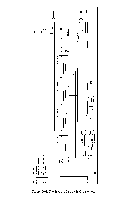
the busses.
Fortunately, it is possible to enormously simplify the
layout of the elements through two techniques:
- serializing the connections, which reduces the size
of the busses to a single line, and
- hard-wiring the transition rules, which does away
with the need for a look-up table.
These techniques, while not applicable to all cellular
automata, are extremely useful for our automaton which, as we mentioned,
was designed for exactly this kind of hardware implementation.
The resulting circuit (Fig. B-4) consists
of four D-type flip-flops, a few logic gates, and four 1-bit-wide connections
(inputs from the south and west neighbors, outputs to the north and east
neighbors). Its operation, because of the hard-wired transitions, is not
apparent at first glance, and requires some explaining.
The configuration stream for the automaton (Fig.
3.29) is stored in an EEPROM (Electrically-Erasable Programmable Read-Only
Memory) outside of the array, and enters the array from the lower left
corner element. The four possible states of the automaton are encoded using
three bits:
|
State
|
Encoding
|
|
Horizontal wall
|
001
|
|
Spare column
|
011
|
|
Vertical wall
|
101
|
|
Junction
|
111
|
Table B-1: Encoding of the states of the automaton.
The states enter the array left-bit-first, so that the
first bit of each state is always a 1. Each element receives information
indifferently from the south or the west inputs. As long as the element
receives only 0s, nothing happens, and the automaton remains in
the quiescent state 0000. As the first
1arrives, it is
stored in the first flip-flop ( Q3), and shifted from there to
the second ( Q2) and the third ( Q1). At this point, when
Q1=1
(since the first bit of an incoming state is always 1) and Q0=0
(since the element has not yet been configured), the automaton makes a
decision:
- if Q3=0(that is, if the incoming state
is either a horizontal wall or a spare column) and the data is coming in
from the south and not from the west, then the incoming state is ignored
and the flip-flops reset, since horizontal walls and spare columns should
only propagate horizontally;
- if Q3=1and
Q2=0(that is, if the
incoming state is a vertical wall) and the data is coming in from the west
and not from the south, then the incoming state is ignored and the flip-flops
reset, since vertical walls should only propagate vertically;
- in all other cases, the flip-flops are not reset
and the incoming state is allowed to shift once more, so that Q0=1
and Q1and Q2uniquely identify the state of the element.
Once the element is configured (Q0=1), the shift
chain is broken: Q2, Q1, and
Q0remain fixed, thus
setting the state of the element, while the incoming stream passes through
Q3
and is propagated to the north (if the state is a vertical wall or a junction)
and/or to the east (if the state is a horizontal wall, a spare column or
a junction). The state itself is then decoded to provide the required signals
which are used to redirect the flow of the FPGA's configuration.
This small circuit allows the user to very simply define
rectangular membranes of any given size and to program the frequency and
placement of the spare columns, and is thus functionally equivalent to
the automaton described in subsection 4.3.3.
B.1.3 The Self-Repair Level
Immediately below the cellular automaton level we find
a level dedicated to the rerouting of the connections for self-repair (Fig.
B-5).
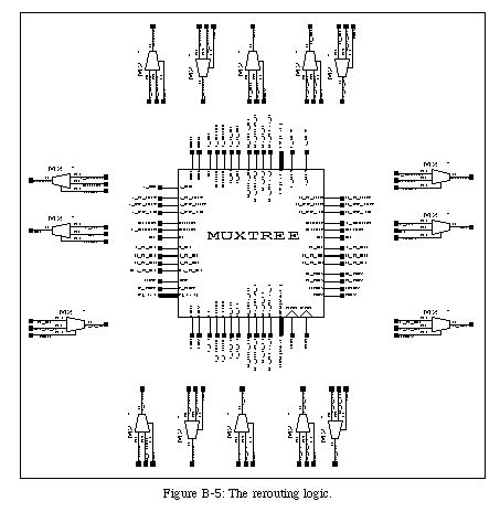
As we have seen in chapter 4,
our self-repair mechanism reconfigures the array so as to avoid using the
faulty elements, and reroutes the connections around them. The minimal
set of connections that need to be rerouted to implement the pattern shown
in Fig. 4.17 consists of:
- on the north side, the input and output long-distance
busses NIBUSand NOBUS, the short-distance output NO, and the input and output configuration lines C_NIand C_NO
(that is, the lines used to propagate the configuration through all the
elements in a block);
- on the south side, the input and output long-distance
busses SIBUSand SOBUS, the short-distance input SI, and the input and output configuration lines C_SIand C_SO;
- on the west side, if the element is active the
output long-distance bus WOBUSreceives the corresponding output
of the internal switch block and the short-distance output WOreceives
the short-distance input SI, while if the element is dead, WOBUS
receives the input long distance bus
EIBUSand WOreceives
the short-distance input EI;
- on the east side, if the element is active the
output long-distance bus EOBUSreceives the corresponding output
of the internal switch block, the short-distance output EOreceives
the short-distance input SI, and the output configuration line
C_EO
receives the signal generated within the element, while if the element
is dead, EOBUSreceives the input long distance bus
WIBUS, EOreceives the short-distance input WI, and C_EO
receives the input configuration line
I_C_WI;
In addition, we put at this level one extra multiplexer
whose function is to connect the global configuration line GL_C_O
to the west input configuration line I_C_WIin entry point elements.
Placing the multiplexer at this level is not strictly necessary, but simplifies
the layout.
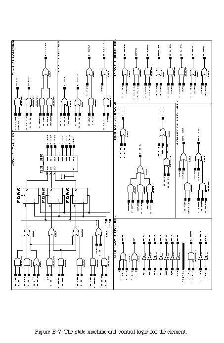
B.1.4 The Control Logic
Figure B-6 shows the core of the MuxTreeSR
element. The three main subcircuits described in chapter
4 (the programmable function, the switch block, and the configuration
register) are clearly visible. Also visible is a fourth subcircuit, labeled
STATE, which has not so far been described.
 In this subcircuit (Fig. B-7), we
collected all of the control logic required to handle all the phases of
the operation of our array. Its size, while consequent, is not quite as
important as it might appear, since it also includes a considerable amount
of logic required for the operation of the Biodule (logic which would then
disappear in a VLSI implementation). Moreover, some of the signals generated
in this subcircuit are required not by the system itself, but rather by
the use of a Xilinx FPGA, which is somewhat limited in its versatility
and has some peculiar requirements which complicate the design of our control
system (for example, it has difficulty handling bidirectional busses crossing
multiple chips, a non-trivial problem where our global control lines are
concerned).
In this subcircuit (Fig. B-7), we
collected all of the control logic required to handle all the phases of
the operation of our array. Its size, while consequent, is not quite as
important as it might appear, since it also includes a considerable amount
of logic required for the operation of the Biodule (logic which would then
disappear in a VLSI implementation). Moreover, some of the signals generated
in this subcircuit are required not by the system itself, but rather by
the use of a Xilinx FPGA, which is somewhat limited in its versatility
and has some peculiar requirements which complicate the design of our control
system (for example, it has difficulty handling bidirectional busses crossing
multiple chips, a non-trivial problem where our global control lines are
concerned).
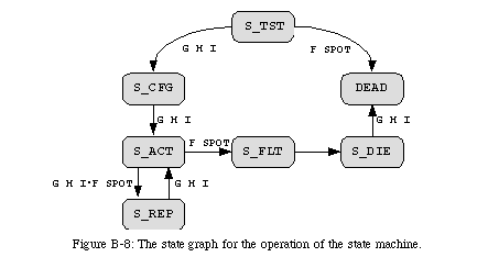
 The heart of the control logic is a state machine, implementing the state graph of Fig. B-8. Each element
of the array can be in one of 7 possible states, and the transitions are
controlled by two signals:
The heart of the control logic is a state machine, implementing the state graph of Fig. B-8. Each element
of the array can be in one of 7 possible states, and the transitions are
controlled by two signals:
- A global hold signal
G_H_I. This signal
is used to "freeze" the execution of the circuit. It can be seen as a single
global line which is usually pulled to 0by a pull-down resistor
outside the array. Any element can pull it to 1by setting the G_H_O
signal. It is set to 1while the register is being tested, while
the configuration bitstream is propagating, and while the reconfiguration
mechanism is active.
- An internal fault detection signal F_SPOT. This signal is set to 1if and only if a fault is detected inside
the element itself.
The seven states operate as follows:
- S_TST( 000) is the initial state.
In this state, the element is waiting for the test pattern (
subsection 4.2.5 ) to come in and check the register, and
imposing a 1on G_H_O. If a fault is spotted during this
test, the element immediately dies ( DEAD). If, on the other hand,
no fault is spotted, the global hold signal is released. As soon as all
the elements have released the hold signal ( G_H_I=0), the element
starts to wait for the configuration to arrive ( S_CFG).
- S_DIE( 001) is the state acquired
by the faulty element while the repair process is occurring. As soon as
the reconfiguration is complete ( G_H_I=0), the element dies (
DEAD).
- S_FLT( 010) is a temporary state,
introducing a one-clock-cycle delay between the detection of a fault and
the beginning of the repair process. It is not in fact required for the
operation of the array, but is a consequence of certain limitations of
the Xilinx chip, and should disappear in a VLSI implementation.
- S_REP( 100) is the state acquired
by all non-faulty elements during the repair process. The elements go back
to the active state ( S_ACT) as soon as the reconfiguration is
finished.
- S_CFG( 101) is the configuration
state. Elements remain in this state while they are waiting for the array
to be configured. In this state, they pull the global hold line to 1
as long as their configuration register is not full. Once configured, they
release the global hold line. Once the global hold line goes to 0
(i.e., when all the elements have been configured), the array begins operation
and all elements go to state S_ACT.
- S_ACT( 110) is the active state.
All elements, once configured, remain in this state and execute their function
until the circuit is reset or the repair mechanism is activated.
- DEAD( 111) is the state of faulty
elements after the reconfiguration is complete. Elements in this state
are not part of the operation of the array, and the only exit from this
state is through a global reset of the FPGA.
Among the other signals generated in this subcircuit,
we will mention:
- G_K_O, a semi-global signal which propagates the
KILL
command (subsection 4.3.5) throughout a
column of blocks;
- R_COL_O, which propagates downwards
the information that the column contains spare elements;
- R_C_EO, which is set to 1if
the current element is or has been involved in the repair process;
- R_C_WO, which is set to 1 to signal
the completion of the repair process;
- V_DEVand H_DEV, which control
the rerouting of the connections;
- REG_EN, which enables the shifting of
the array, either during the configuration phase or during the repair process;
- REG_RST, which resets the configuration
register.
Apart from the above, the subcircuit also contains some
intermediary control signals and some control logic for the 7-segment displays
in the Biodule.
B.1.5 The Programmable Function
The subcircuit implementing the programmable function
(Fig. B-9) is a straightforward implementation of the
layout shown in Fig. 4.14. It consists
of two copies of the original function plus some test logic.
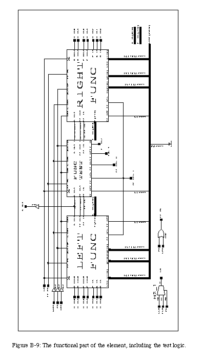
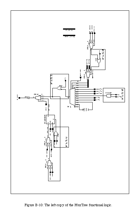
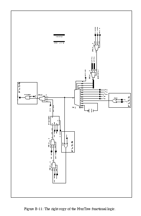
The left (Fig.B-10) and the right
(Fig.B-11) copies are identical, except for the different
positioning of the faults. The layout corresponds exactly to the one shown
in Fig. 4-2, with the exception of a slightly
modified input selector, which nevertheless performs the same function.
Note the relatively complex control logic for the flip flop, required to
allow it to be set to a default value stored in the configuration (
FF_DEF) and to be chained with the configuration register ( FF_CFG
).
As far as the test logic is concerned (Fig.
B-12), it is a direct implementation of the circuit described in subsection
4.2.3, with the comparator for fault detection, the third copy of the
flip-flop, and the 2-out-of-3 majority function FF_OUT.

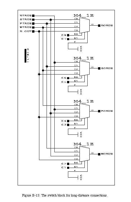
B.1.6 The Switch Block
There is not much to say about the switch block (Fig.
B-13), which is a straightforward implementation of the circuit described
in subsection 4.1.2. It allows any one
of the four output busses to carry the signal coming from the three other
input busses or the output N_OUTof the element.
B.1.7 The Configuration Register
The hardware implementation of our configuration register
led us to one relatively important modification to the propagation mechanism
for the bitstream. This modification (which in no way alters our overall
approach) concerns the mechanism which fills the registers with the appropriate
value.
In the mechanism we described in chapter
4, the registers within a block were chained together to form one long
shift chain. This approach, while perfectly feasible, requires however
a dedicated global line to signal the end of the block's configuration,
as well as some relatively important amount of additional logic to detect
such an event.
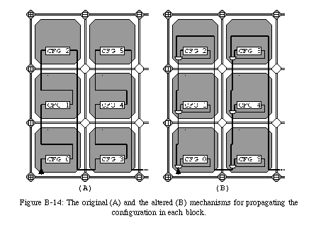
In order to avoid this penalty, we altered our mechanism
so as to fill the registers in order (Fig. B-14): rather
than filling all registers in series, we fill the first, then the second,
and so on until the last in the block. The new mechanism does away with
the need to detect and propagate the end of the configuration at the expense
of an additional bit in the configuration register. In fact, with this
approach we require a way to detect that a register has been completely
filled, so as to proceed to the next. We found that the least expensive
way to obtain such behavior was to set the first (head) bit of the configuration
of each element to 1: the end of the configuration is then signaled
by the arrival of the 1to the head of the register.
Aside from this modification, the implementation of our
configuration register (Fig. B-15) is identical to
the design introduced in chapter 4. The register,
which in this implementation is 24-bit wide40, receives its configuration from one of three possible sources:
- if the array is expecting the test sequence
of subsection 4.2.5 to arrive, all the
registers will receive it in parallel from the global configuration line;
- if the element is on the bottom row of a block,
or if the element is undergoing reconfiguration, the input will come from
the west input line41;
- if none of the above conditions is true, than
the register will receive its configuration from the south input line.

Once the register is full ( C0=1), the propagation
path is fixed according to the patterns of
Fig.
4.5:
- the output line to the north propagates the
input line from the south unless the element is in the bottom row of the
block, in which case it propagates the input from the west, or an entry
point, in which case it propagates the global configuration line;
- the output line to the south propagates the
input line from the north unless the element is in the top row of the block,
in which case it propagates the input from the south input line;
- during configuration, the output line to the
east propagates the input line from the north in all cases, while during
self-repair it is used to shift the configuration of an element to its
east neighbor.
Finally, the register subcircuit of Fig.
B-15 contains the test logic described in subsection
4.2.5, slightly augmented to handle some Xilinx-related issues.
B.2 MuxNet
As we have seen, the Biodule 603 is the main hardware
prototype we realized in order to test the validity of our mechanisms.
However, the size of the circuit required to implement a single MuxTreeSR
element prevents us from realizing systems which require more than a few
logic elements. In the long term, we hope to overcome this difficulty through
the realization of a dedicated VLSI circuit which will contain an important
number of elements. In the short term, however, such a solution is not
available to us.
To obtain a larger number of programmable elements, we
investigated the possibility of exploiting a system based on an array of
Xilinx FPGAs mounted on a single printed circuit board and configured so
as to implement an array of MuxTreeSR elements. Such a system, while far
from allowing the same density as a VLSI chip, would nevertheless allow
us to obtain a much larger number of elements than an array of Biodules,
particularly if we were not limited to a single MuxTreeSR element for each
Xilinx chip.
The first step in the design of this system was therefore
an analysis of the number of MuxTreeSR elements we can fit into a single
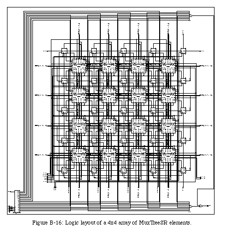
Xilinx FPGA. To this end, we defined a layout consisting of a 4x4 array
of our logic elements (Fig. B-16). Without attempting
major optimizations in the layout of the elements42, we removed the logic dedicated exclusively to the Biodule displays, and
tried to determine the smallest Xilinx FPGA capable of containing the whole
array. Running our design through the Xilinx routing software, we determined
that the smallest FPGA which can hold the entire array is a XC4025HQ240.
A system based on an array of such chips could thus allow us to obtain
a fairly large array of MuxTreeSR elements, and indeed would be an interesting
intermediate step in the creation of our VLSI circuit, likely to be realized
as soon as we arrive at a quasi-definitive version of our FPGA.
40.The extra bits are unused in the
current implementation, but were introduced in view of possible future
alterations in the design.
41.Note that the special case of
the entry points was taken care of at the self-repair level (subsection B.1.3).
42.The optimal solution to this
kind of design would be to create a "hard macro" of a MuxTreeSR element,
that is, define by hand the configuration of the circuit. Such a solution,
however, would be extremely time-consuming.